Published 2024-10-26
This will be a fairly short article, but I wanted to touch on some work I have done recently with the tool OpenEMS. OpenEMS is a free and open-source electromagnetic field solver. It’s an extremely capable tool, though it requires quite the learning curve. I’ve intended to learn OpenEMS for over a year now and have just finally got around to it.
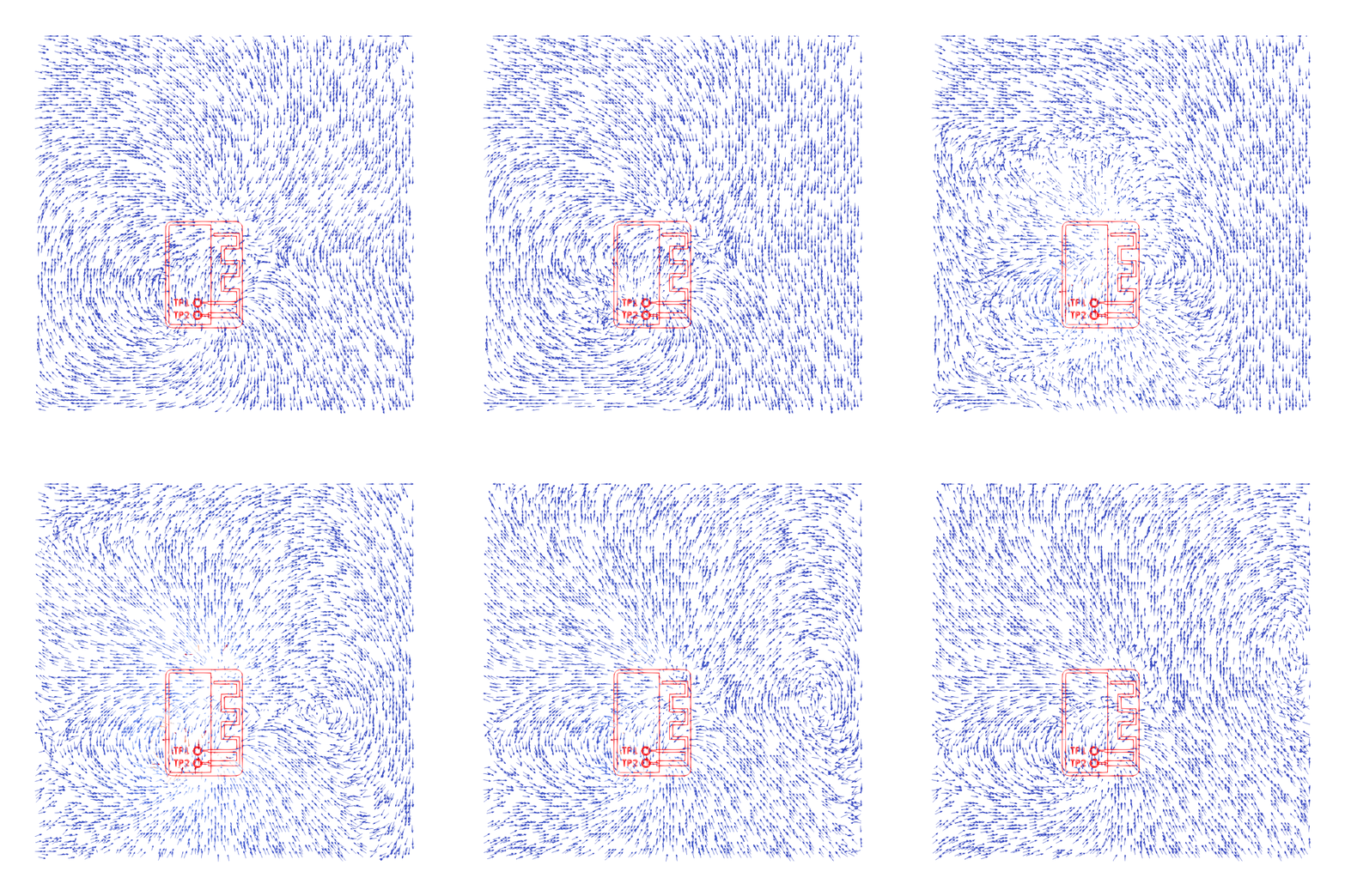
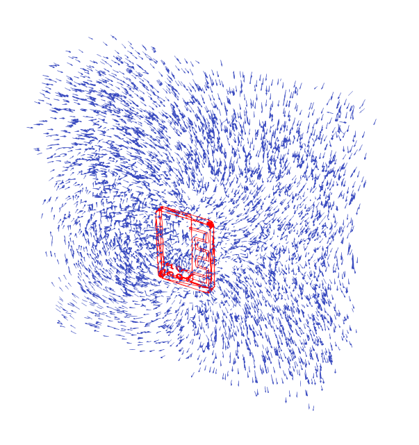
Below is an animation I produced of the electric field around a 2.4 GHz meandering inverted-F antenna design1. I designed the PCB in KiCAD and wrote a short script to convert an exported DXF layer into a perfect electric conductor (PEC) polygon in OpenEMS. (A method loosely inspired by this article.) This appeared to be the simplest way to produce the copper geometry I wanted, and one where I would have the option to produce a full simulation pipeline in the future if I so desire. The current state of the art for importing PCBs into openEMS seems pretty poor, so writing my own script felt like an appropriate option.
The final simulation required some tweaking to achieve. This is the first time I have designed a mesh for an FDTD by hand but is necessary for OpenEMS, fortunately some debugging quickly found where I was going wrong. Placing the part within the simulation also proved challenging due to a lack of a well defined origin in my exportation method. The results below were rendered with Paraview and animated with GIMP. OpenEMS does require additional configuration to export electric field data over-time with the use of an electric field “dump” (just in case anyone wishes to replicate this kind of experiment). I should note that the location of the antenna I have drawn on in the figure below is only approximate. (See my comment about a lack of common origin, this is the greatest limitation in my current approach to simulation.)


The future work I’d like to complete with OpenEMS would be somewhat more practical. Chief in my mind is investigating high-speed signals on PCBs. I would quite like to see the impact of different transmission line geometries impacts the characteristic impedance of a trace as well as the impacts of different stackups on signal integrity and electromagnetic emissions.
Footnotes
-
A. Andersen, “Small Size 2.4 GHz PCB Antenna,” Texas Instruments, https://www.ti.com/lit/an/swra117d/swra117d.pdf ↩